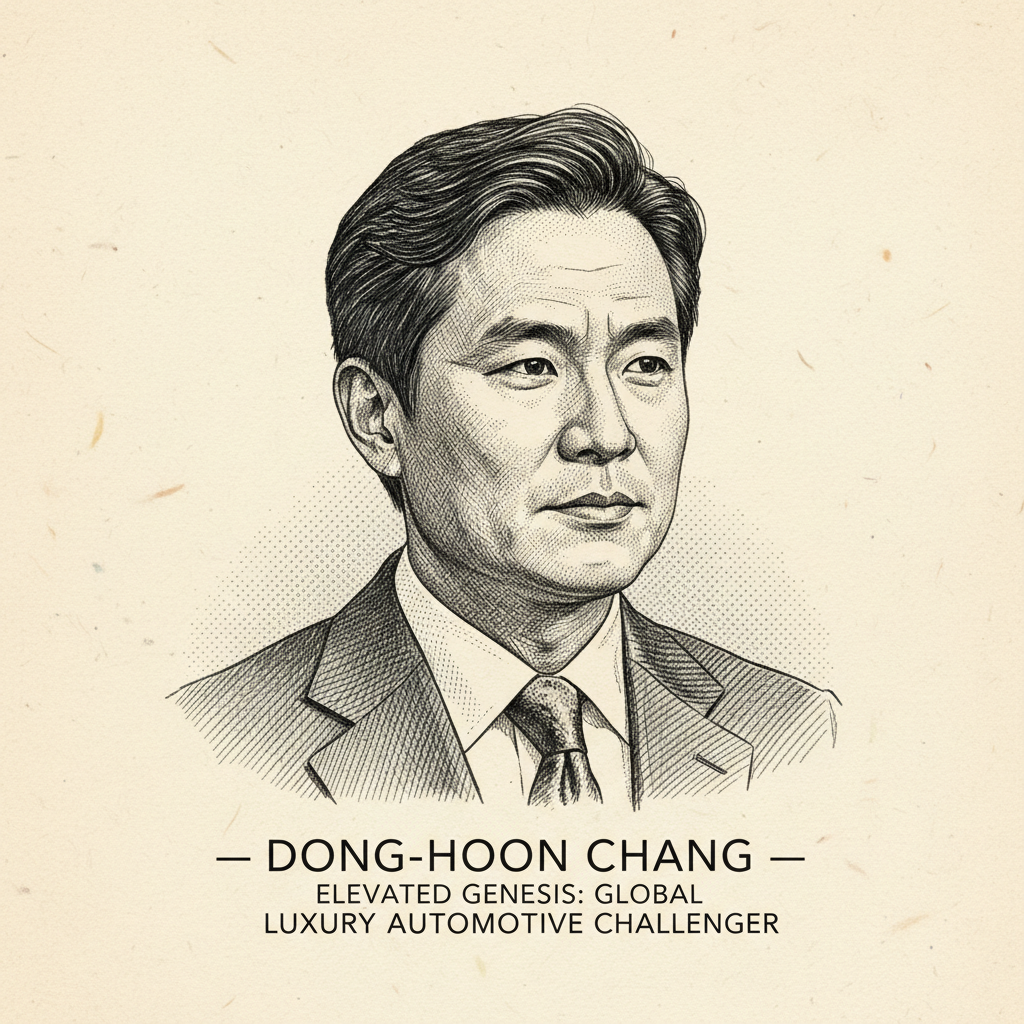
Sang-Hyun Lee
Architecting advanced semiconductor packaging to accelerate next-generation memory and AI solutions.
Sang-Hyun Lee leads the critical Packaging & Test division at SK Hynix, a global leader in memory semiconductors. His leadership is instrumental in developing and scaling advanced packaging technologies, such as High Bandwidth Memory (HBM), which are pivotal for AI, high-performance computing, and data center infrastructure. He navigates complex manufacturing challenges to ensure product quality, cost efficiency, and timely delivery of cutting-edge memory solutions.
Biography
Accomplishments
- 01Spearheaded the mass production of HBM3 at SK Hynix, establishing the company's early lead in the critical high-bandwidth memory market (e.g., 2022).
- 02Directed the development and successful rollout of HBM3E (Enhanced HBM3), pushing the boundaries of memory performance for AI and HPC applications (e.g., 2023-2024).
- 03Implemented advanced packaging technologies, such as Through-Silicon Via (TSV) and hybrid bonding, significantly enhancing memory density and data transfer rates.
- 04Optimized packaging and test operations, contributing to SK Hynix's improved yield rates and cost efficiency across its DRAM and NAND product lines.
- 05Established robust quality control protocols within the P&T division, ensuring the reliability and longevity of advanced semiconductor products in demanding environments.
Lessons for Operators
Key Takeaways
Practical lessons distilled for operators, investors, C-levels, and capital allocators.
Packaging as a Core Competence
For semiconductor manufacturers, packaging has evolved from a back-end process to a core strategic competence. Investment in R&D and manufacturing capabilities for advanced packaging (e.g., HBM 3D stacks, chiplets) directly translates to market share in high-growth segments like AI and HPC.
Yield and Quality Define Profitability
In highly competitive memory markets, small improvements in packaging and test yield can significantly impact profitability. Rigorous process control and data analytics are essential to maximize output and minimize defects for complex products.
Alignment with Ecosystem Partners
The success of advanced memory technologies like HBM is deeply intertwined with collaboration with CPU/GPU manufacturers and system integrators. Early engagement ensures that packaging solutions meet specific system-level performance and integration requirements.
Operational Scalability for New Tech
Transitioning from R&D to mass production for novel packaging technologies demands robust operational planning and scalable manufacturing infrastructure. Challenges in scaling HBM production underscore the need for early investment in industrialization.
Frameworks & Principles
Named frameworks and strategic principles they popularized or embodied.
Design for Manufacturing (DFM) for Advanced Packaging
Integrating manufacturability considerations early in the packaging design phase to optimize for yield, cost, and reliability. This includes considerations for material selection, assembly processes, and test methodologies.
When to useApplicable during the initial design and development phases of new semiconductor packages, especially for complex 3D structures like HBM or chiplet integration.
Statistical Process Control (SPC) in Packaging & Test
Utilizing statistical methods to monitor and control manufacturing processes to ensure that they operate within their desired capabilities, thereby reducing variability and preventing defects.
When to useContinuously applied across all high-volume packaging and testing lines to maintain quality standards, identify process shifts, and implement corrective actions proactively.
Total Quality Management (TQM) principles for Semiconductor Quality
A management approach to long-term success through customer satisfaction, focusing on continuous improvement, employee involvement, and a process-centered system in all aspects of manufacturing, including packaging and test.
When to useAdopted as an overarching organizational philosophy to foster a culture of quality and continuous improvement throughout the entire packaging and test lifecycle, from initial design to final product delivery.
Explore Related Titans
Other figures in the archive who share Sang-Hyun Lee's domain, geography, or era.
More in Technology









From South Korea